
In this post, I will show the plasmonics. It is an emerging field that leads with plasmons, which are electron waves generated by light.
How to create plasmons?
When light focuses in a dielectric “sandwich” with two metals, the dielectric cavity compresses the light signal and the free electrons in the metals oscillate in resonance forming electron waves. Those oscillations are called plasmons which have a defined wavelength.
Plasmons also can be generated on the surface. Inserting a light in an ultra-thin film made of gold with a glass substrate creating the Surface Plasmon Resonance (SPR) phenomena.

The plasmon detection is made by optical sensors that capture the intensity of reflected light in relation to the angle, the light must stay at an angle that makes sure total internal reflection.

Plasmons can only be generated in nanostructures and last very short time.
The Lycurgus Cup
Although the term plasmonics is new, ancient artifacts used the plasmonics principle. The Lycurgus Cup, a Roman glass from 4th century A.D., has gold and silver nanoparticles, probably were put accidentally. The glass stays red when a source of light is put inside and green when light is reflected in it.
Plasmonic circuits
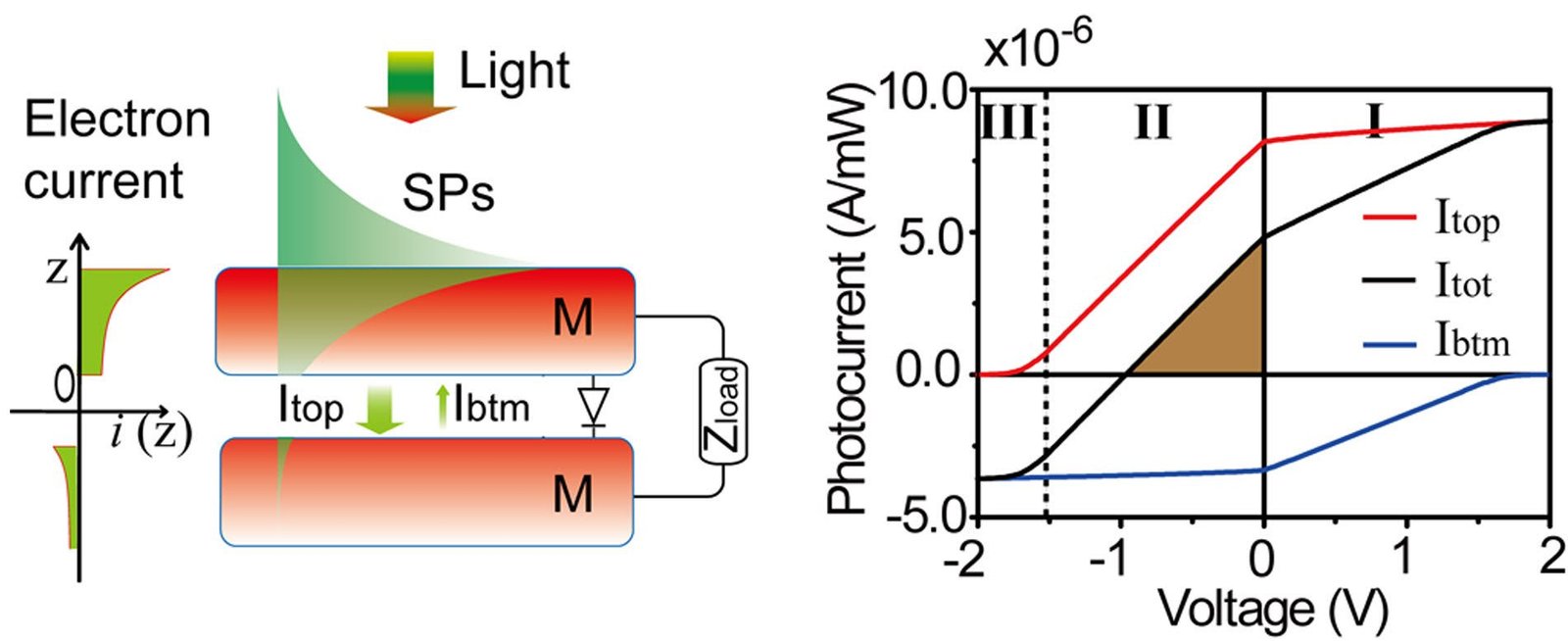
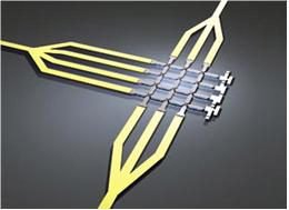
The speed of chips and microprocessors can be greatly increased with plasmons conductors because these can transport a great quantity of information, combining the high speed of light with microelectronic’s miniaturization. Here we have a surface plasmon detector that converts optical signals into electricity.
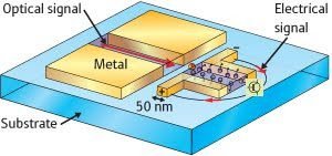
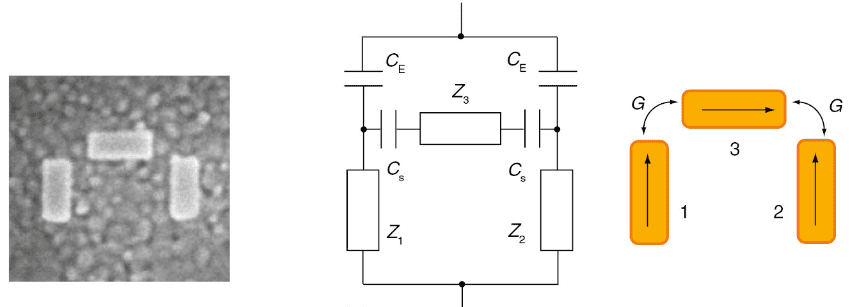
In the device above, two nano pieces in L form with a germanium layer and generates an electrical current. Other plasmonic structures have the electronics equivalent if receive light in a determinate wavelength. This 100 nm length gold nanorod behaves like a RLC circuit.

These nanorods arranged like this behave like a circuit bridge.
To build plasmonic computers, it is necessary to build a component equivalent to the transistor to the plasmonics. This device is the plasmonster, it has a guide wave slot to receive light.
When receives light in the guide wave, the plasmonster creates electron waves in a frequency. Generating electrical current which can control electronic devices, operating like a key similar to the transistor.
Application in medicine
One of the promises in this area in medicine is cancer treatment without collateral effects. Inserting 100 nm silica nanospheres with 10 nm gold coat.
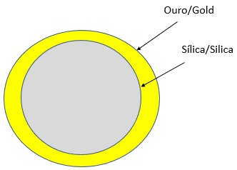
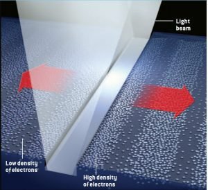
These nanoparticles will be inserted in a tumor area, when receiving infrared light, electrons oscillate and kill cancer cells without destroying the good ones.
Stealth

Another fascinating promise is the possibility to create materials that enter in resonance with the light, making the refraction index equal to the air, therefore invisible. Something saw until now only in movies like the Predator and games like Command & Conquer and Metal Gear Solid.


The structure would absorb light, but a material that amplifies the optical signal with a spacer would compensate for the loss by absorption and metamaterials could theoretically redirect electromagnetic waves.
Others aplications
Others possible applications of plasmonics:
- Solar cells;
- Silicon LEDs;
- Spacer, plasmons laser;
- Nanoantennas;
- Raman spectroscopy;
- Ultrasensitive sensors;
- Scanning Tunneling Microscopy.