In this post I will explain how the BJT (Bipolar Junction Transistor) works. Exist many other types of transistors which will stay to other posts. This is one of the most important electronic components.
Structure
The bipolar junction transistor (BJT) has two types of layer structure: NPN in the right and PNP in the left.

As I explained in the post about diodes, the P layer is silicon doped with an element which has 3 electrons in the last layer (usually boron). While N is silicon doped with an element which has 5 electrons in the last layer (usually phosphorus). To know more about diodes click in this button.
 DiodesClick here
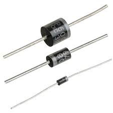
These diodes won’t work as transistors, because there is metallic wire between the middle layers.

Representation of BJTs in circuit schematics, NPN in the left and PNP in the right.

Operation as key
As you can see, the middle layer linked to the base terminal is much thinner. The transistor needs two voltage signals to work. Let’s considerate the NPN type.

When the VBE voltage is zero, there is no current flux, because a transistor’s junction will always be in the reverse mode. In this situation it is said that the transistor is in cutoff. When the VBE reach a voltage high enough to surpass the potential barrier of the junction between base (B) and the emitter (E), which usually is 0,7 V, generate a current in the base (the middle terminal). Many electrons from the emitter will be attracted by the P material of the collector.

The result is that a small current in the base can control a bigger current which flux from the collector to the emitter like a key. The emitter current (Ie) is the sum of the currents of the base (Ib) and the collector (Ic).
Ie=Ic+Ib
When there is current from the collector to the emitter, it is said that the transistor is in saturation. If was the PNP type, the transistor will stay in cutoff with the current in the base and in saturation without it and the voltage direction of VCE have to invert. In practice, this circuit below is one of the forms to use the transistor as a key.

Every BJT transistor have a parameter called \beta or h_{fe} which determine how much the collector current is amplified in relation to the base current.
\beta=\frac{Ic}{Ib}
Operation as amplifier
Exist an operation mode of the BJT beyond cutoff and saturation. It is the active mode, in this region the transistor is used to amplify signals without distortion. This graphic shows the typical characteristic curve of the BJT transistor.

Here is the graphic of the characteristic curve to a NPN bc548 transistor from Micro Electronics.

And this is of the PNP bc558 transistor from Fairchild Semiconductor. The values vary depending of the manufacturer and the code.

To a transistor be used as an amplifier, it must be polarized with resistors in a way that the Ic and the voltage between collector and the emitter (Vce) stays in the amplification region. The polarization (resistors calculation) techniques stay to another post.
I have learn some just right stuff here. Certainly value bookmarking for revisiting. I surprise how much attempt you set to make such a magnificent informative web site.
Hello, Neat post. There is a problem together with your site in internet explorer, might test this… IE still is the marketplace leader and a huge portion of folks will omit your fantastic writing because of this problem.
I use the Internet Explorer and I have no problem in access.
I was more than happy to find this web site. I need to to thank you for ones time just for this wonderful read!! I definitely loved every part of it and i also have you saved as a favorite to look at new information on your website.
I simply want to tell you that I am just newbie to blogging and certainly savored your blog. Very likely I’m going to bookmark your blog post . You certainly have exceptional posts. Regards for sharing your website page.