
In this part about MEMS manufacturing, the subject is surface micromachining. A very different method from the one shown in previous part.
Surface micromachining for MEMS
This is an additive or bottom-up method, are deposited thin material layers in silicon substrate for microparts construction.
Substrate and sacrificial layer
In silicon substrate the sacrificial layer is implemented. Has this name because it’s removed after micropart’s construction. Usually, the material of sacrificial layer is silicon oxide, deposition and removal of this layer have already been explained in part 1, whose link is at the beginning of post.

Polysilicon
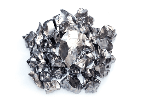
The most used material to make microstructures for MEMS is polysilicon or polycrystalline silicon. Polysilicon is a material with silicon crystals with many sizes.

Polycristalline silicon has a very high purity degree. As a semiconductor, can be applied in microsensors. One of reasons to use is the convenience, because this material is applied in manufacturing of MOSFETs for chips. Polysilicon also is used in fabrication of photovoltaic panels.
Polysilicon deposition
How is the polysilicon structural thin film placed? The method is LPCVD (Low Pressure Chemical Vapor Deposition), the surfaces (wafers) are placed inside a quartz or silica tube in a inductive or resistive heater. Gas is injected by a mass flow controller system. In schematics, the equipment at right of tube, serves to control pressure inside the tube with mechanical pumps, keeping tube interior at low pressure.
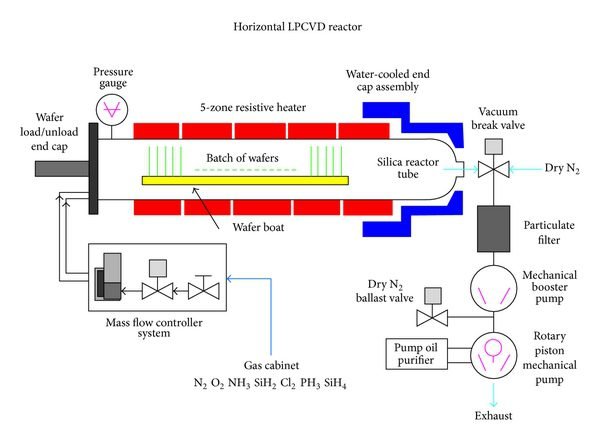

One of injected gas to produce polysilicon film is the silane (SiH_4), the following chemical reaction is produced with temperature between 580ºC (1076ºF) and 850ºC (1562ºF). Deposition rate is between 60 and 200 Å/minute (Å is read as ångström and 1 Å=1\cdot 10^{-10}m).
SiH_{4}\rightarrow Si+2H_{2}
Another gas which can be used to polysilicon deposition is disilane (Si_{2}H_{6}).
Si_{2}H_{6}\rightarrow 2Si+3H_{2}
This reaction is made with temperature between 450ºC (842ºF) and 550ºC (1022ºF). Deposition rate between 4 and 1360 Å/minute.

The crystalline silicon’s shape in MEMS is made by photolithography, it will be subject to a future post.
Removing sacrificial layer
The last stage of surface micromachining is removal of sacrificial layer with hydrofluoric acid.
SiO_{2}+4HF\rightarrow SiF_{4}+2H_{2}O
An illustration of all typical stages of surface micromachining.

When more complex the MEMS project, bigger the number of structural and sacrificial layers.
Why silicon?
Exist many other alternative materials for substrate, structural and sacrificial layers. Why is silicon the most used material to MEMS manufacturing? The reasons are:
- Abundance: Silicon can be extracted from sand.
- Familiarity with manufacturing of silicon substrate.
- High melting point: 1400ºC.
- High Young module (resistance to elastic deformation): Between 130 and 187 GPa, this value depends on crystalline structure.
- Low thermal expansion coefficient in comparison with other materials, whose value is: 2,6\cdot 10^{-6} C^{-1}.