
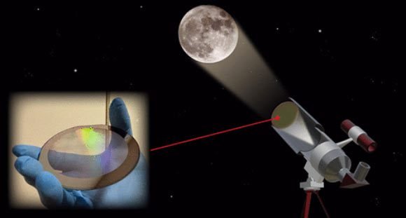
Was developed the metalens, a new type of lens for telescopes and cameras, which can be flat and operates on near-infrared region.
Source: SciNews
“Traditional camera or telescope lenses have a curved surface of varying thickness, where you have a bump in the middle and thinner edges, which causes the lens to be bulky and heavy,” said Dr. Xingjie Ni, a researcher at the Pennsylvania State University.
“Metalenses use nano-structures on the lens instead of curvature to contour light, which allows them to lay flat.”
Metalenses are typically made using electron beam lithography, which involves scanning a focused beam of electrons onto a piece of glass, or other transparent substrate, to create antenna-like patterns point by point.
However, the scanning process of the electron beam limits the size of the lens that can be created, as scanning each point is time-consuming and has low throughput.
To create a bigger lens, Dr. Ni and colleagues adapted a fabrication method known as deep ultraviolet (DUV) photolithography, which is commonly used to produce computer chips.
“We found this to be a good fabrication method for metalenses because it allows for much larger pattern sizes while still maintaining small details, which allows the lens to work effectively.”

The researchers modified the method with their own novel procedure, called rotating wafer and stitching.
They divided the wafer, on which the metalens was fabricated, into four quadrants, which were further divided into 22 by 22 mm regions — smaller than a standard postage stamp.
Using a DUV lithography machine, they projected a pattern onto one quadrant through projection lenses, which they then rotated by 90 degrees and projected again.
They repeated the rotation until all four quadrants were patterned.
“The process is cost-effective because the masks containing the pattern data for each quadrant can be reused due to the rotation symmetry of the metalens,” Dr. Ni said.
As the size of the metalens increased, the digital files required to process the patterns became significantly larger, which would take a long time for the DUV lithography machine to process.
To overcome this issue, the scientists compressed the files using data approximations and by referencing non-unique data.
“We identified identical data points and referenced existing ones, gradually reducing the data until we had a usable file to send to the machine for creating the metalens.”
Before the technology can be applied to modern cameras, however, they must address the issue of chromatic aberration, which causes image distortion and blurriness when different colors of light, which bend in different directions, enter a lens.
“We are exploring smaller and more sophisticated designs in the visible range, and will compensate for various optical aberrations, including chromatic aberration,” Dr. Ni said.
The team’s work was published in the journal Nano Letters.


