
The shift register is useful for increase the number of the microcontroller’s output terminals and to convert parallel binary data in serial and vice-versa.
What is a shift register?
It’s a set of connected flip-flops in a way that can store and transfer binary data. A flip-flop transfer bits to the next one at each clock pulse. The output of a sequential circuit is connected to the input of another.
In case you don’t know what are flip-flops, read the post about the subject before continue.
An application example of shift register is in electronic calculators, where a number is moved to the left when you press another number key.
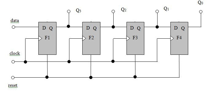
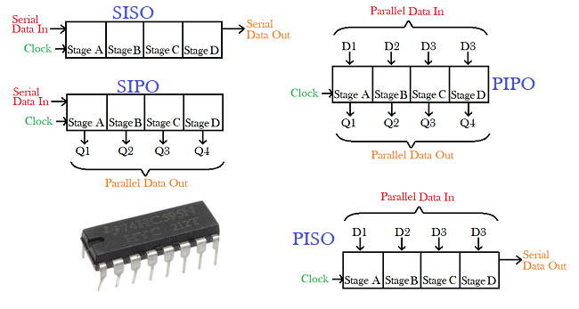
Parallel and serial
The registrators types are divided accoding to inputs and outputs.
Ring counter
The output of the last flip-flop is linked to the first’s input.
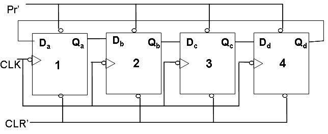
In this circuit, the output pattern is repeated for each determined number of pulses, equal to number of flip-flops. For example, if there are 4 flip-flops, the pattern will repeat at every 4 pulses.
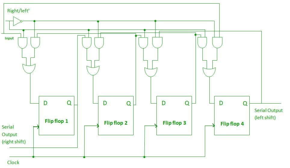
Bidirectional shift register
Some integrated circuits can transfer data in both directions, depending on configuration. Have combinational circuits, input to determine the transfer direction, and two outputs: one for each direction.
Integrated circuit 74HC595
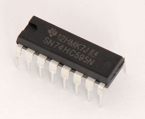
This is one of the most popular circuits for projects involving shift register. Has 8 bits (1 byte) SIPO, CMOS technology, uses type D flip-flops, and voltage range from 2 to 6 V.
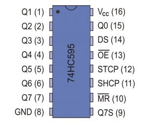
Explaining the function of each chip’s terminal.
- Vcc (16) is supply pin and GND (8) is ground.
- Q0 (15) to Q7 (7) are flip-flop’s outputs.
- Q7S (9) is the serial output.
- SHCP (11) is the shift register clock input.
- DS (14) is serial input.
- OE (13), input enable.
- STCP (12), storage register clock, also knows as latch.
- MR (10), master reset.
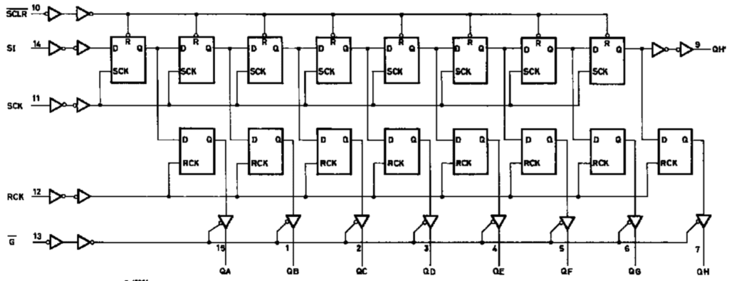
Inside the 74HC595, there are 8 flip-flops which are the shift register, the other 8 are the storage register. Each output (QA for QH) has a buffer, amplifier with gain 1. The buffer doesn’t amplify signal but serves to control charges with a higher power, isolating it from lower power logic doors.
Project with 74HC595 and Arduino
In this project, 16 LEDs are controlled with only 3 Arduino terminals. Connecting 2 cascade 74HC595.
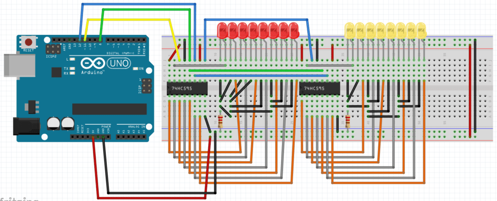

For this project, you need to download the library ShiftOut.h, click here.
#include <ShiftOutMega.h>

int number=0;
//Variáveis de uso dos registradores 74HC595
int latchPin = 8;  //Pin 12 connected to pin 12 of 74HC595 (Latch).
int dataPin = 11;  //Pin 13 connected to pin 14 of 74HC595 (Data).
int clockPin = 12; //Pin 11 connected to pin 11 of 74HC595 (Clock).

//Quantity of registers (74HC595).
int qtdRegistradores = 2;

//LED vector
byte leds[]={1,2,3,4,5,6,7,8,9,10,11,12,13,14,15,16};
//Variable that detects direction.
int direction=1;
int returnled=15;

ShiftOutMega mega(latchPin, dataPin, clockPin, qtdRegistradores); //Initiate library passing usage parameters.

void setup(){
  Serial.begin(9600);
}

void loop(){
  //Initialize all LEDs as low.
  for(int i=0;i<16;i++){
    mega.shiftWrite(leds[i],LOW);
  }
  //Turns on the first LED.
  mega.shiftWrite(leds[number],HIGH);
  number += direction; //Follows a direction.
  if(number==16){  //If arrives to the last, changes direction.
    direction=-1;
  }
  if(number==0){ //If arrives at the first, changes direction.
    direction=1;
  }
}


Expanded my culture what a wonderful subject very good post wonder.
Your website is amazing congratulations, visit mine too:
https://strelato.com
.