
The MOSFET is another type of field effect transistor. Much more used than JFET and it’s the most important component for digital computers.
This is the link to access the post about junction field effect transistor.
Structure
In addition to three terminals: gate, source and drain, MOSFET has the body terminal. In some transistors, body is linked to the source.
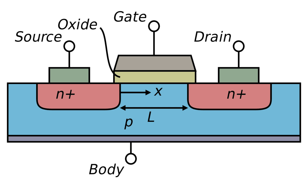
MOSFET (Metal oxide semiconductor field effect transistor) has this name due to small insulating film made of silicon oxide (SiO_{2}), put between the gate’s conductor material and substrate. The conductor electrode is made of polycrystalline silicon or polysilicon and doped with high impurity degree.

Due to SiO_{2} insulating layer, this device’s input impedance is higher than JFET.
Types of MOSFETs and operation
In addition to n and p types, the MOSFETs can be divided in other two categories: enhancement and depletion types. They have different operation modes.
Enhancement type MOSFET or E-MOSFET

Applying a difference potential between source and drain, there will be no current circulation on MOSFET. Because there are p-n junction and one of them is on reverse polarization, blocking the current. Gate’s polysilicon, oxide and semiconductor form a MOS capacitor, that generates an electric field when MOSFET receives a positive potential on gate, if its a nMOS.
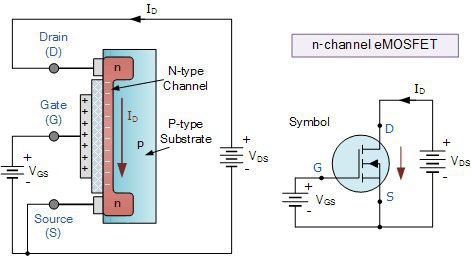
Due to induced channel, there will be current circulation between drain and source. If it were a pMOS, polarities of V_{GS} and V_{DS} would have to be inverted.

The relation between current drain (I_{D}) and V_{GS}.
I_{D}=k(V_{GS}-V_{T})^2
Where k is a constant related to component construction. Can be calculated as follows:
k=\frac{I_{D(ON)}}{\left (V_{GS(ON)}-V_{T} \right )^{2}}
I_{D(ON)} and V_{GS(ON)} can be found on transistor’s datasheet.Depletion type MOSFET or D-MOSFET
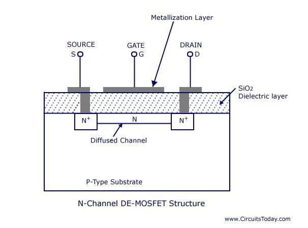

Despite the name, it can work on depletion and enhancement mode. Depends on the voltage V_{GS}. When there is no potential on gate and a voltage between drain and source, the current I_{DSS} circulates through the channel.

If potential on gate is positive, electrons are attracted and holes are repelled. Making the channel expand, increasing current until a limit determined by V_{GS}. Must watch the maximum drain current the component can handle.
